After SMT components are placed & QC’ed, the next step is to move the boards to DIP production to complete through hole component assembly.
DIP = dual in-line package, is called DIP, is an integrated circuit packaging method. The shape of the integrated circuit is rectangular, and there are two rows of parallel metal pins on both sides of the IC, which are called pin headers. The components of the DIP package can be soldered in the plated through holes of the printed circuit board or inserted into the DIP socket.
1. Suitable for through-hole soldering on PCB
2. Easier PCB routing than TO package
3. Easy operation
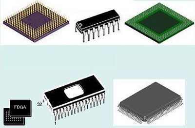
2. The Application of DIP:
CPU of 4004/8008/8086/8088, diode, capacitor resistance
3. The Function of DIP:
A chip using this packaging method has two rows of pins, which can be soldered directly on a chip socket with a DIP structure or soldered in the same number of solder holes. Its feature is that it can easily achieve through-hole welding of PCB boards and has good compatibility with the motherboard.
4. The Difference between SMT & DIP
SMT generally mounts lead-free or short-lead surface-mounted components. Solder paste needs to be printed on the circuit board, then mounted by a chip mounter, and then the device is fixed by reflow soldering.
DIP soldering is a direct-in-package packaged device, which is fixed by wave soldering or manual soldering.
5. The difference between DIP & SIP
DIP: Two rows of leads extend from the side of the device and are at right angles to a plane parallel to the component body.
SIP: A row of straight leads or pins protrudes from the side of the device.