PCB assembly(PCBA) is the process of creating a printed circuit board (PCB) by attaching electronic components to a PCB. There are two main types of PCB assembly: surface-mount technology (SMT) and through-hole technology (THT).
SMT(surface-mount technology)
In SMT, electronic components are mounted directly onto the surface of the PCB using a soldering process. This method is ideal for small, lightweight components and allows for a high degree of automation, making it a cost-effective solution for mass production.
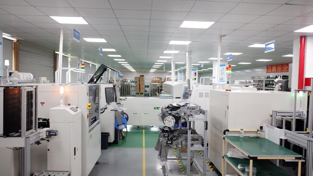
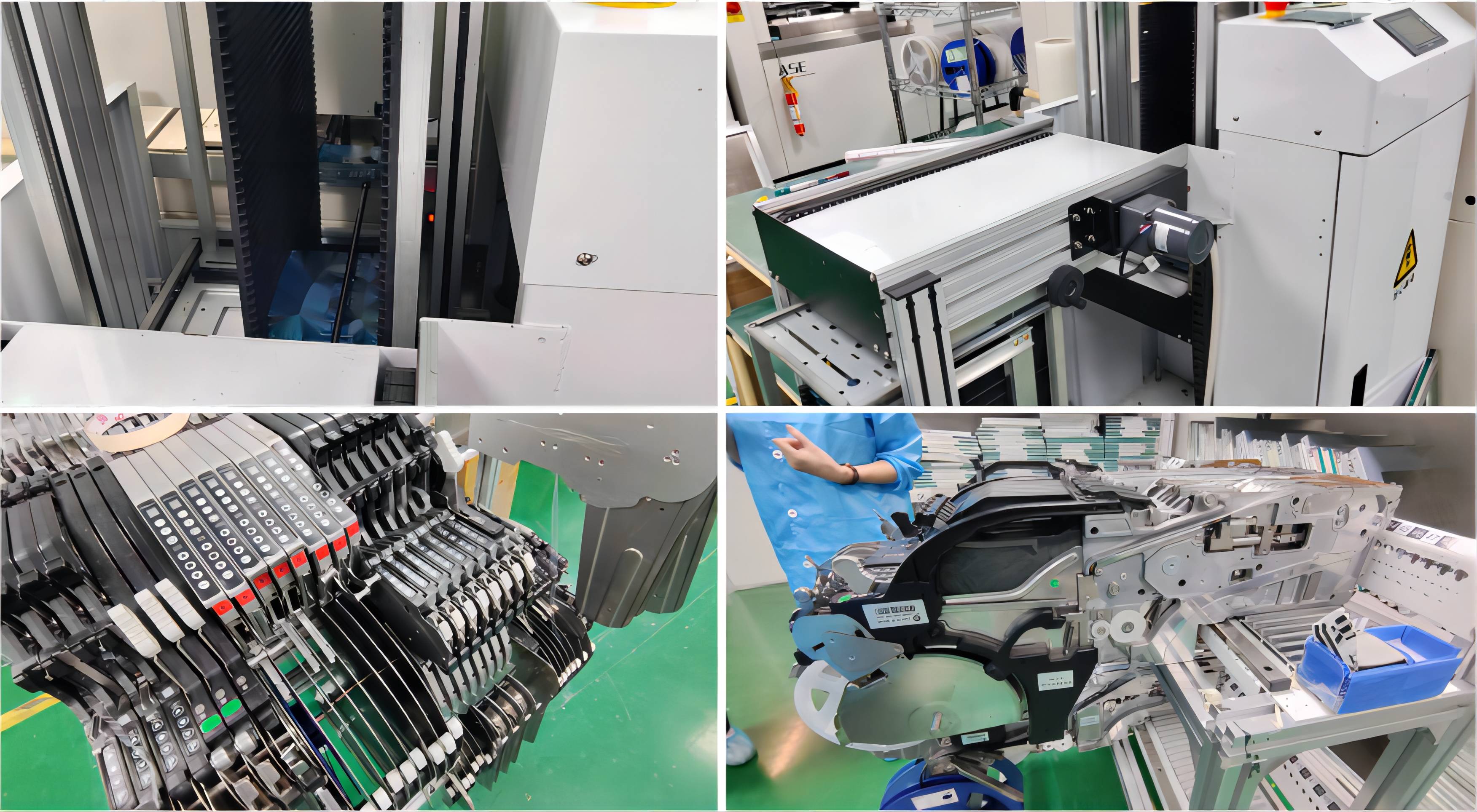
In the automatic assembly line of Fumax, as shown in the figure below, the automatic board loader is used to transport PCB to the solder paste printer; The automatic feeder is widely used to improve the efficiency of component placement.
THT(through-hole technology )
THT, on the other hand, involves inserting the leads of electronic components through holes in the PCB and soldering them to pads on the other side. This method is typically used for larger components and offers a stronger connection, making it suitable for applications where reliability is critical.
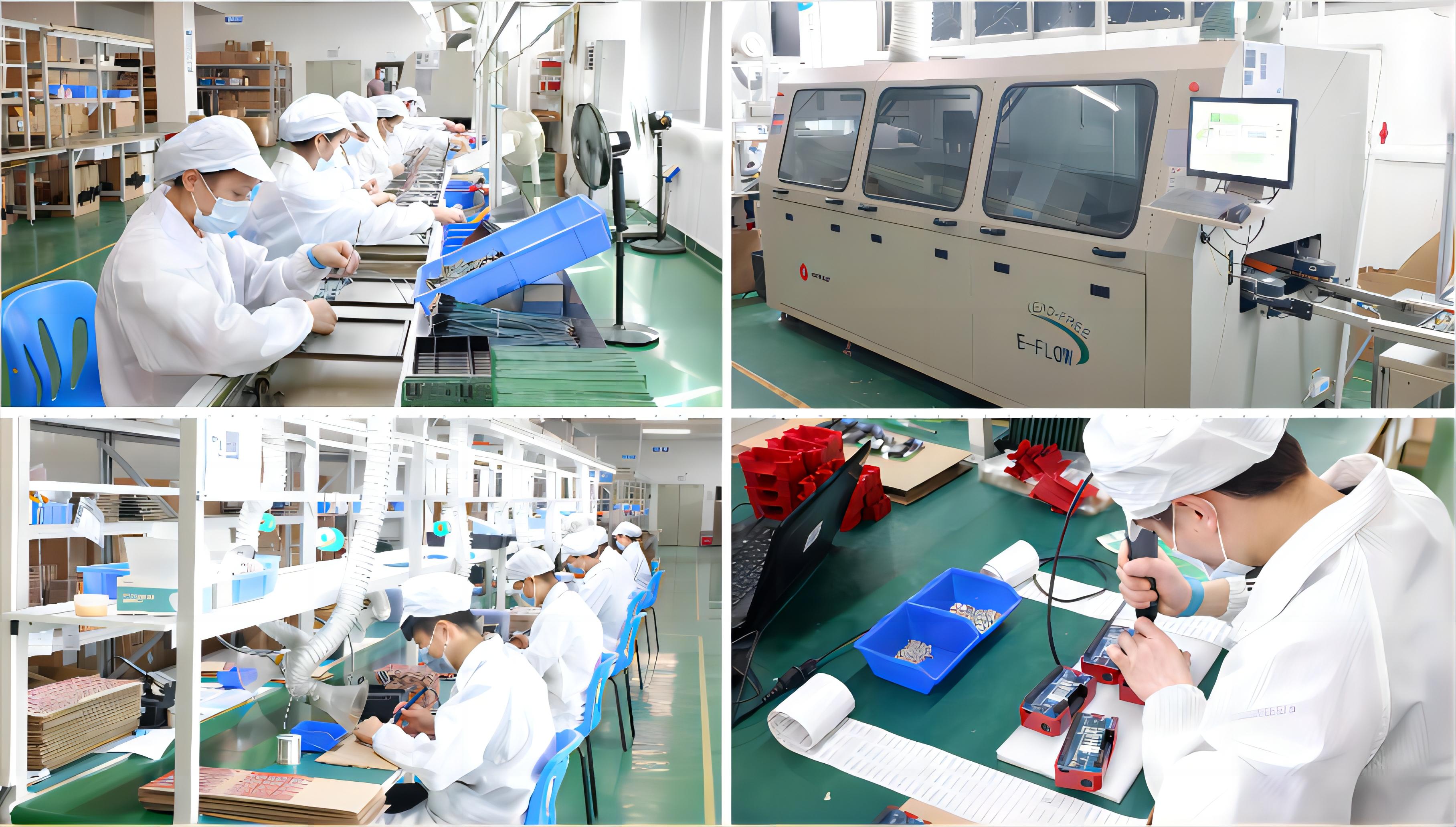
At Fumax, PCBS with attached components are sent to the DIP production line, where skilled workers complete the remaining DIP components and even finished product assembly. In addition, we will also use wave soldering equipment to improve efficiency. Click here to learn more about Fumax wave soldering equipment!
PCBA Quality Control
During the PCBA process, quality checks are performed at each step to ensure that the finished product meets the required specifications. Since Fumax is a ISO:9001 certificated factory, we has a complete and strict quality control system.For example,components are only purchased from authorized suppliers and conduct quality tests on all incoming materials.
As it’s known that PCB bare board is the brick of everything, Fumax build ICT for each board to test board connection and functions. ICT is known as in-circuit test, here we build customized testing fixture for each board!
In the process of circuit board assembly, SPI,AOI and X-ray(for BGA packaged component) are the key quality checking methods.
SPI(soldering paste inspection) is an SMT testing device that uses the principle of optics to calculate the solder paste height printed on the PCB by triangulation. It is the quality inspection of solder printing and the verification and control of printing processes.
AOI(automatic optical inspection) is a detection device with a high-speed moving camera. The board to be tested is placed under the camera and scanned in few seconds, by comparing with the parameters of the standard sample, to ensure accurate placement of components.
BGA package chip has become more and more common nowadays, the special ball pin makes its soldering quality can not be directly detected by visual inspection. So Fumax uses X-ray equipment to take perspective images of BGA chips on PCBS to see if they are well soldered.
In the end of the production, all pcbas in Fumax will be functional tested before shipping, based on customer’s testing procedure. A special testing fixture will be built for each project to improve effective.
Fumax production scope
As a one-stop manufacturer, Fumax provides high quality PCBA services. Our PCB assembly capabilities are as follows:
| Supported Capabilities | |
| Types of Assembly | SMT (Surface-Mount Technology) |
| THD (Thru-Hole Device) | |
| SMT & THD mixed | |
| Double sided SMT and THD assembly | |
| SMT capability | PCB layer: 1-32 layers; |
| PCB material: FR-4, CEM-1, CEM-3, High TG, FR4 Halogen Free, FR-1, FR-2, Aluminum Boards; | |
| Board type: Rigid FR-4, Rigid-Flex boards | |
| PCB thickness: 0.2mm-7.0mm; | |
| PCB dimension width: 40-500mm; | |
| Copper thickness: Min:0.5oz; Max: 4.0oz; | |
| Chip accuracy: laser recognition ±0.05mm; image recognition ±0.03mm; | |
| Component size: 0.6*0.3mm-33.5*33.5mm; | |
| Component height: 6mm(max); | |
| Pin spacing laser recognition over 0.65mm; | |
| High resolution VCS 0.25mm; | |
| BGA spherical distance: ≥0.25mm; | |
| BGA Globe distance: ≥0.25mm; | |
| BGA ball diameter: ≥0.1mm; | |
| IC foot distance: ≥0.2mm; | |
| Component Package | Reels |
| Cut tape | |
| Tube and tray | |
| Loose parts and bulk | |
| Board shape | Rectangular |
| Round | |
| Slots and Cut outs | |
| Complex and Irregular | |
| Assembly process | Lead-Free (RoHS, REACH) |
| Design file format | Gerber |
| BOM (Bill of Materials) (.xls,.CSV, . xIsx) | |
| Coordination (Pick-N-Place/XY file) | |
| Electrical testing | AOI (Automated Optical Inspection), |
| X-ray Inspection | |
| ICT (In-Circuit Test)/ Functional testing | |
| Reflow Oven profile | Standard |
| Custom |
For summary, Fumax Tech provides rapid and reliable turnkey Electronic Contract Manufacturing (EMS) services.The typical PCB assembly process are below, we aim to be your most reliable partner in China!
Simply email your BOM files (Bill of Materials) and Gerber files to us at sales@fumaxtech.com, we will get back to you within 24 hours.
It is needed that BOM includes the quantities, reference designators, manufacturer name and manufacturer part number. Gerbers needs to include the PCB requirements.